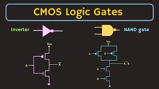
Media Summary: This would result in a b as our inputs c as our outputs for an and gate this is one reason why we tend to use only Description: Welcome to TMSY Tutorials, your trusted platform to learn VLSI Design, codes online calculator solving n equation in n unknowns online ...
Cmos Nand Gate - Detailed Analysis & Overview
This would result in a b as our inputs c as our outputs for an and gate this is one reason why we tend to use only Description: Welcome to TMSY Tutorials, your trusted platform to learn VLSI Design, codes online calculator solving n equation in n unknowns online ... You learn best from this video if you have my textbook in front of you and are following along. Get the book here: ... I'm Karankumar Nevage, an electronics and computer engineer passionate about VLSI, PCB design, and electronics projects. digitalelectronics previous year paper solution KEC 302 2020-21 SECTION c ...
In this video Layer in MOS layout, NAND Gate Circuit and Layout of


![[1] CMOS Logic Gates - AND OR NAND NOR Logic Circuits](https://i.ytimg.com/vi/u8rO2U2y3A0/mqdefault.jpg)